TSMC Might Cut 3nm Prices to Lure AMD, Nvidia
TSMC Might Cut 3nm Prices to Lure AMD, Nvidia
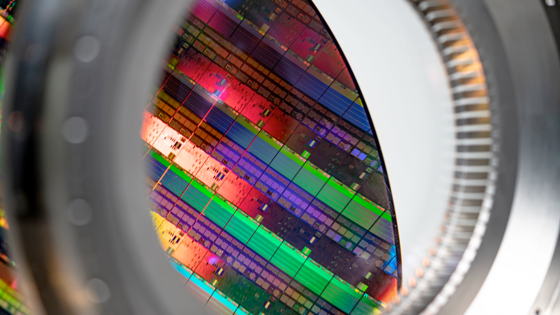
Although TSMC’s N3 (3nm-class) family of fabrication processes brings a number of benefits in terms of performance and power, the very high costs of the foundry’s initial N3 node hampers widespread adoption. Unsurprisingly, the company is rumored to be preparing to lower its quotes for 3nm production to stimulate interest from chip designers, according to a report from MyDrivers.
While at this point any published TSMC’s N3 quotes and prices should be considered rumors, it’s likely that TSMC’s production costs on its N3E process will be lower than those on its initial N3. It remains to be seen how much the company will charge for production on other N3-class nodes, such as N3P, N3S, and N3X. Lowering prices of 3nm production will attract more customers to these nodes, but this is not something that is going to happen overnight.
TSMC’s initial N3 manufacturing technology (also known as N3B) is rumored to be used only by Apple because the company is the foundry’s largest client willing to adopt leading-edge nodes ahead of others. But N3 is an expensive technology to use. N3 extensively uses extreme ultraviolet (EUV) lithography for up to 25 layers, according to China Renaissance, and each EUV scanner now costs $150 million – $200 million, depending on configuration. To depreciate fabs equipped with such production tools, TSMC has to charge more for production on its N3 process and successors.
Some say that TSMC might be charging as much as $20,000 per N3 wafer — up from $16,000 per N5 wafer — and while such quotes depend on numerous factors, the key takeaway is that chip production keeps getting more expensive. Increased costs mean lower profits for companies such as AMD, Broadcom, MediaTek, Nvidia, and Qualcomm, which is why chip developers are reconsidering how they create advanced designs and use leading-edge nodes.
“We believe the meaningful [N3] ramp-up will be in 2H 2023 when the optimized version, N3E, will be ready,” wrote Szeho Ng, an analyst with China Renaissance. “Its major customers in HPC (i.e., AMD, Intel), smartphone (i.e., QCOM, MTK) and ASIC (i.e., MRVL, AVGO, GUC) will likely stay in N4/5 and choose N3E as their maiden N3 class foray, in our view. Meanwhile, we believe the baseline N3 (aka N3B) adoption will be largely limited to Apple products.”
To stimulate its partners into using its N3-class process technologies, TSMC is reportedly considering lowering its quotes for these nodes. In particular, TSMC’s N3E process uses EUV only for up to 19 layers and features somewhat lower complexity in terms of manufacturing, and is thus cheaper to use. TSMC could lower quotes of N3E production without harming profitability. N3E provides zero advantages over N5 when it comes to SRAM cell scaling, which means larger die sizes when compared to those made on N3/N3B.
AMD publicly announced that it planned to use an N3 node for some of its Zen 5-based designs due in 2024, and Nvidia is expected to adopt N3 for its next-generation Blackwell architecture-based GPUs set to arrive around the same timeframe. Due to high costs, adoption of N3-class nodes is expected to be limited to certain products — so lowering quotes will probably make chip designers reconsider their adoption strategy.
There’s also another issue with TSMC’s N3: low yields. Some estimate yields are between 60% and 80%, and sources at DigiTimes (via Dan Nystedt) indicate that they’re below 50%. That said, since only Apple reportedly uses this manufacturing technology and the company is known for being very secretive, any details about yields of initial N3 chips should be taken with a large grain of salt.